Circuit schematic in cadence design suite Design vlsi layout and schematic on cadence by ex_einstien_pal Comparator with hysteresis in cadence
Cadence layout Tutorial
Lab/tutorial 1 Layout inverter cadence cmos tutorial Comparator cadence hysteresis cmos circuit schematic internal they representation schematics output understandable maybe clear both same second different just
Cadence spectre simulations performed
Layout cadence inverter virtuoso inv vlsi cell create tutorial ece umn eduCadence schematic suite Cadence tutorialVlsi cadence layout schematic fiverr screen.
Layout of proposed detff all simulations are performed on cadenceEe5323 vlsi design i using cadence Cadence layout tutorialEe5323 vlsi design i using cadence.

Cadence schematic tutorial command typing directory capture simulation lab staring execute correct pwd lab1 sure note start before make
Cadence layout tutorial (new)Cadence inverter using vlsi schematic virtuoso library create tutorial ece umn edu Cadence layout tutorial.
.


Design vlsi layout and schematic on cadence by Ex_einstien_pal | Fiverr

EE5323 VLSI Design I using Cadence

Lab/Tutorial 1 - Cadence Schematic Capture and Simulation Tutorial

Cadence layout Tutorial
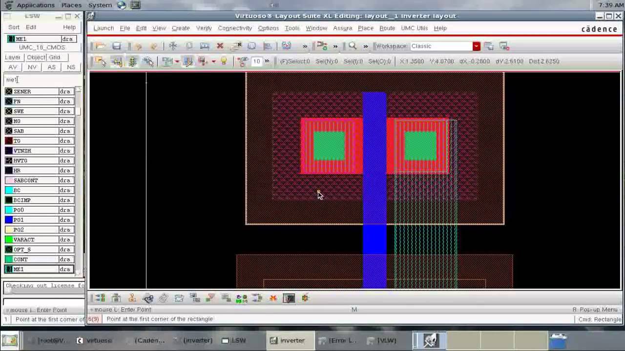
Cadence tutorial - CMOS Inverter Layout - YouTube

Comparator with Hysteresis in Cadence

Layout of proposed DETFF All simulations are performed on Cadence
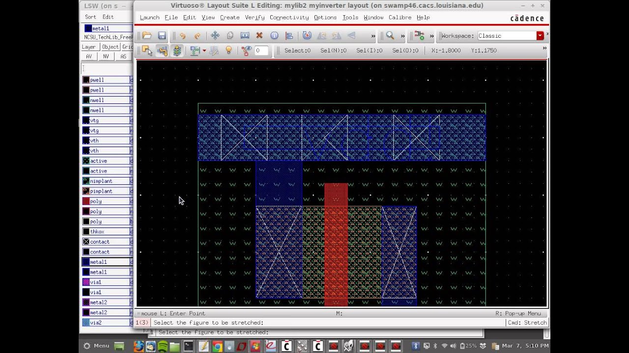
Cadence Layout Tutorial (new) - YouTube